Signal Chain Design Considerations for the Data-Hungry World

Image Source:
Anterovium/shutterstock.com
By Mark Patrick, Mouser Electronics
Published February 11, 2020
With the emergence of the Internet of Things (IoT), leveraging high-performance computing in the cloud and on
edge platforms, the applications we use to run everything from our personal wellness and mobility to the homes
and offices we occupy all have a greater appetite for data. Thanks to this data, society is becoming smarter.
We are monitoring aspects of the physical environment around us through an increasing number and variety of
sensors. These sensors generate signals that are often of low amplitude and inherently noisy. Often they will
contain non-linearities and, in the majority of cases, they need to be converted from their real-world analog
form into computer-ready digital values. Each signal chain that purifies and converts those raw measurements, so
as to bridge from the sensor to the compute/processing resource, has a crucial role in giving life to the data
demand.
Common Signal Chain Features
Generically speaking, a signal chain will comprise certain key elements. These are namely the sensor (or data
acquisition hardware), signal amplification and filtering, followed finally by an analog-to-digital-converter (ADC) to sample and digitize the conditioned signal for
subsequent processing or storage.
One or more amplifier stages might be required—such as a trans-inductance amplifier (TIA) followed by a
voltage-gain amplifier. In addition, multiple filters might be needed to isolate the signal chain to within a
certain frequency range, implement anti-aliasing for high-frequency signals and eliminate unwanted signals at
specific frequencies (e.g. interference from the AC mains supply). Depending on the sensor's output it might
make sense to amplify the signal before filtering, understanding that any noise will thus also be amplified.
Alternatively, filtering can be applied first.
A successive approximation register (SAR), or sigma-delta ADC, might be best suited to the task of digitizing the
filtered and amplified signal. SAR ADCs tend to have lower latency than sigma-delta devices, although the
maximum sample rate is typically lower. Strengths of sigma-delta ADCs include high resolution and strong power
efficiency, and additional features (such as filters, multiplexers, or input buffers) are often also integrated.
Figure 1: Generic signal chain components. (Source: Mouser Electronics)
Use Case of Industrial Temperature Monitoring
Temperature is said to be the most commonly monitored aspect of the physical world. A thermocouple can detect
extremely high temperatures in industrial applications, but the output voltage is small (typically only a few mV). The
signal chain components (as shown in Figure 2) must ensure high amplifier gain with low noise
and low drift.
A reference temperature must also be monitored to provide cold junction compensation (CJC), allowing the
instrument to generate an output voltage corresponding to the temperature sensed at the thermocouple probe. CJC
is often implemented using either a resistance temperature detector (RTD) device or a silicon-based temperature
sensor. An RTD requires an excitation voltage, which the signal chain design utilized must provide.
Thermocouples, RTDs, and thermistors all display inconsistent linearity that must be
corrected somehow within the signal chain. As far as thermocouples are concerned, the change in output voltage
for a given change in temperature is determined by the Seebeck coefficient. Because this coefficient is not
constant across the thermocouple's operating temperature range, it is best to choose a type that offers the most
linear response possible across the temperature range in which it will be working. For this, design engineers
can refer to Institute of Printed
Circuits (IPC) categories that standardize the properties of various types of thermocouples. As an
example, an IPC type S thermocouple offers a useful temperature range from about 0°C to 1500°C and
displays reasonable linearity from about 900°C to 1250°C. Reference tables for standard thermocouple
types, such as those published by the American National Institute of Standards and Technology (NIST), enable
linearity to be corrected digitally, saving the complexity of linearity correction within the signal chain
itself.
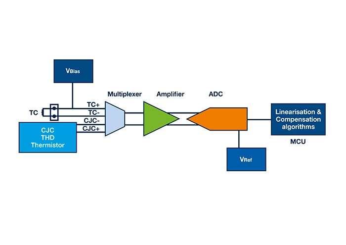
Figure 2: An example of a thermocouple signal chain. (Source: Mouser
Electronics)
Because each physical electrical connection to the thermocouple unavoidably creates an additional thermojunction,
care must be taken to ensure that all connections except the temperature sensing probe and the cold junction are
the same temperature.
Use Case for Medical/Fitness Monitoring
With the growing desire for self-quantification, as well as faster, more cost-effective healthcare, there is demand for
easier sensing of bio-indicators (such as body temperature, blood oxygen, and heart rate) using either
clinical-grade instruments or consumer-type devices (such as wristband trackers). Compared to thermistors and
RTD temperature sensors, which require substantial signal processing, silicon-based temperature sensors offer
greater linearity, stability, and ease of use. Although they have a narrower temperature range (typically from
-20°C to 70°C), this is more than adequate for body-temperature monitoring by medical devices and
wearables.
Maxim's MAX30208
is a clinical-grade digital temperature sensor that is optimized for straightforward, non-invasive
body-temperature measurement. The temperature level is measured at the top of the package—which is
easiest to place against the skin surface and least affected by self-heating issues (because of supply current
entering via the IC pins). Pinning is optimized to allow mounting on a flexible printed circuit that can be
positioned remotely from the host processor, and the I2C interface allows daisy-chaining of multiple
sensors to capture data at several points on the body for optimum accuracy. The MAX30308 measures body
temperature to within ±0.1°C and contains integrated signal chain circuitry and a 32-bit FIFO to
simplify interaction with the host processor.
As far as monitoring heart activity is concerned, clinical-grade monitors have traditionally relied on
electro-cardiographic (ECG) signals from multiple sensors attached to the body. More recently, optical
photo-plethysmographic (PPG) sensing has developed to provide acceptable accuracy from a small, non-invasive
wearable device—such as a fitness wristband or finger-clip pulse oximeter. PPG sensing works by
transmitting light through body tissue and measuring the reflected or transmitted signals. Small changes in
blood volume can be quantified, enabling indicators (including blood oxygen saturation, heart rate, and
respiration) to be calculated. It is also possible to make inferences about tissue condition and organ fucntion.
The voltage signal from a PPG instrument's optical sensors contains a DC component related to blood volume and
the optical properties of bone and tissue, with an AC component caused by changes in blood volume that
correspond to the heartbeat. Other small signals generated by activity (such as respiration) are also present.
Designing the signal chain for a wearable heart-rate monitor begins with the transmitter, which can be a green
LED or a combination of red and infrared LEDs. the wavelength and intensity of the source determine the depth of
penetration and received signal strength, and can be adjusted for optimum accuracy. On the other hand, LED
drivers introduce noise to the transmitted signal and power consumption must be considered, too.
The receive-side signal chain has to sample the photodetector output, handle ambient light cancelation, filter
the signal, and do the ADC. The photodetector output is a current signal whose amplitude could be less than a nA
or up to a few tens of μA. A transimpedance amplifier (TIA) is needed to convert the current signal into a
voltage, and the design of the signal chain must take into account factors such as the signal dynamic range,
signal-to-noise ratio (SNR), board utilization, and power consumption associated with elements such as
anti-aliasing filters and the TIA. Fortunately, the large and growing market for wearable consumer-grade
heart-rate monitors means engineers can opt for an integrated analog front end (AFE)—such as the AFE4490 from Texas
Instruments or Maxim's MAX30110/12, which each incorporate the LED driver and a complete photodetector signal
chain within their respective single-chip solutions. These devices provide a convenient mechanism for overcoming
challenges such as manipulating the photodiode current, filtering, buffering, amplification, and converstion
using a sigma-delta ADC.
Use Case in Imaging
Parameters such as human heart rate and industrial process temperatures are relatively simple and stable, placing
only moderate demands on the signal chain as far as speed and sample rate are concerned. The MAX30110/12
supports a sample rate of up to 3.2kSPS—so as to meet the needs of a pulse-oximetry or heart-rate
monitoring application. The signal speeds and sample rates in applications such as image sensing or industrial
machine vision are much greater and require special consideration.
Simple imaging systems, such as near-infrared spectroscopy equipment for inspection or materials analysis, can
employ a linear photodiode that requires cooling to minimize the effects of thermal noise and signal
conditioning. The Analog Devices ADA4807 precision low-noise amplifier has a -3dB bandwidth of 180MHz and is well suited
for use with the company's ADAQ7980 single-chip data-acquisition system that contains a 1MSPS low-noise SAR ADC
with which power scales alongside sampling rate—maximizing efficiency. This device relieves design
engineers of unwanted challenges such as circuit layout and component selection by integrating a high-bandwidth
ADC driver that has low input noise and rail-to-rail output to minimize distortion. The internal power
architecture and provision for an external precision voltage reference also contribute to preserving signal
integrity by lowering system noise.
Machine vision with high-speed cameras and video surveillance applications are placing even grater demands on
signal acquisition. A high-speed frame grabber implements the connection to the camera and interfaces to the
host PC (typically over PCI or PCI Express) using a communication protocol such as Camera Link that defines
video throughput rates from 255Mbps to 680Mbps. The frame grabber also typically implements important video
pre-processing functions—such as gain control, defective pixel compensation, and dynamic range extension.
These often need tbe done at real-time frame rates. Designing a frame grabbber is a significant engineering
challenge, often implemented using FPGAs that provide the signal processing performance required and are also
able to host machine vision algorithms on the same device.
Conclusion
Capturing signals from sensors to create informative data for any application, whether it is consumer,
industrial, or all the way through to medical, requires a good understanding of each of the constituent
components in the signal chain. this covers everything, starting with the sensor and going right up to the ADC,
and in each case the correct items need to be chosen and then properly integrated. In many circumstances, a
single-chip front end is already available, which can effectively simplify design and shorten the
time-to-market.
 Part of Mouser's EMEA team in Europe,
Mark joined Mouser Electronics in July 2014 having previously held senior marketing roles at RS Components.
Prior to RS, Mark spent 8 years at Texas Instruments in Applications Support and Technical Sales roles and holds
a first class Honours Degree in Electronic Engineering from Coventry University.
Part of Mouser's EMEA team in Europe,
Mark joined Mouser Electronics in July 2014 having previously held senior marketing roles at RS Components.
Prior to RS, Mark spent 8 years at Texas Instruments in Applications Support and Technical Sales roles and holds
a first class Honours Degree in Electronic Engineering from Coventry University.
 Türkiye


