


Microchip Technology PIC16F175x Low-Power 8-Bit Microcontrollers (MCUs)

Microchip Technology PIC16F175x Low-Power 8-Bit Microcontrollers (MCUs) are designed to deliver high performance and energy efficiency for a wide range of embedded applications. These Microchip PIC16F175x MCUs feature integrated op amps, high-speed 10-bit Analog-to-Digital Converters (ADCs), 10-bit Pulse Width Modulators (PWMs), and comparators. The MCUs enable precise analog signal conditioning, motor control, and power conversion. With flexible core-independent peripherals and low-power modes, these devices are ideal for use in industrial automation, sensor interfaces, lighting control, and portable devices. A compact footprint and analog integration reduce external component count, simplifying design and lowering system cost.
Features
- Core
- C-Compiler optimized RISC architecture
- Operating speed
- DC to 32MHz clock input
- 125ns minimum instruction time
- 16-level deep hardware stack
- Low-current Power-on Reset (POR)
- Configurable Power-up Timer (PWRT)
- Brown-out Reset (BOR)
- Low-Power Brown-out Reset (LPBOR)
- Windowed Watchdog Timer (WWDT)
- Memory
- Up to 28KB of program Flash memory
- Up to 2KB of data SRAM memory
- Up to 256Bytes of data EEPROM memory
- Memory Access Partition (MAP) with program Flash memory partitioned into:
- Application block
- Boot block
- Storage Area Flash (SAF) block
- Programmable code and write protection
- Device Information Area (DIA) stores
- Fixed Voltage Reference (FVR) measurement data
- Microchip Unique Identifier (MUI)
- Device Characteristics Information (DCI) stores
- Program/erase row sizes
- Pin count details
- Direct, indirect, and relative addressing modes
- Operation
- 1.8V to 5.5V voltage range
- Temperature ranges
- -40°C to +85°C industrial range
- -40°C to +125°C extended range
- Digital peripherals
- 2x Capture/Compare/PWM (CCP) modules
- 16-bit resolution for Capture/Compare modes
- 10-bit resolution for PWM mode
- 2x Pulse-Width Modulators (PWM)
- 16-bit resolution
- Independent pulse outputs
- ERS inputs
- 4x Configurable Logic Cells (CLC), integrated combinational and sequential logic
- 1x Complimentary Waveform Generator (CWG)
- Rising and falling edge dead-band control
- Full-bridge, half-bridge, one-channel drive
- Multiple signal sources
- Programmable dead band
- Fault-shutdown input
- 1x configurable 8/16-Bit timer (TMR0)
- 2x 16-bit timers (TMR1/3) with gate control
- Up to 3x 8-bit timers (TMR2/4/6) with Hardware Limit Timer (HLT)
- 1x numerically controlled oscillator
- Generates true linear frequency control and increased frequency resolution
- Input clock up to 64MHz
- Programmable CRC with memory scan
- Reliable data/program memory monitoring for Fail-Safe operation (e.g., Class B)
- Calculate 32-bit CRC over any portion of Program Flash memory
- 2x Enhanced Universal Synchronous Asynchronous Receiver Transmitters (EUSART)
- RS-232, RS-485, and LIN compatible
- Auto-wake-up on start
- 2x Host Synchronous Serial Ports (MSSP)
- Serial Peripheral Interface (SPI) mode, chip select synchronization
- Inter-Integrated Circuit (I2C) mode, 7/10-bit addressing modes
- Peripheral Pin Select (PPS) enables pin mapping of digital I/O
- Device I/O port
- Up to 35x I/O pins
- 1x input-only pin
- Individual I/O direction, open-drain, input threshold, slew rate, and weak pull-up control
- Interrupt-on-Change (IOC) on up to 25x pins
- 1x external interrupt pin
- 2x Capture/Compare/PWM (CCP) modules
- Package options
- 14-pin PDIP, SOIC, and TSSOP
- 20-pin PDIP, SOIC, SSOP, and QFN
- 28-pin SPDIP, SSOP, and VQFN
- 40-pin PDIP and QFN
- 44-pin TQFP
- Analog peripherals
- Differential Analog-to-Digital Converter with Computation (ADCC)
- Sample rate up to 300ksps
- 12-bit resolution
- Up to 35x external input channels
- 7x internal input channels
- Internal ADC oscillator (ADCRC)
- Operates in Sleep
- Selectable auto-conversion trigger sources
- 2x 10-bit Digital-to-Analog Converters (DAC)
- Buffered output available on up to 2x I/O pins
- Internal connections to ADC, op amps, and comparators
- 1x high-speed comparator (CMP1)
- Configurable power modes for faster response time (50ns) or lower power operation
- Multiple hysteresis selections
- Up to 4x external inputs
- Configurable output polarity
- External output via peripheral pin select
- 1x low-power comparator (CMPLP1)
- Selectable input common mode ranges, including rail-to-rail
- Low operating current
- Up to 4x external inputs
- Configurable output polarity
- External output via peripheral pin select
- Up to 4x operational amplifiers
- Programmable gain using an internal resistor ladder
- Automatic input offset voltage calibration
- 2x Fixed Voltage References (FVR)
- Selectable 1.024V, 2.048V, and 4.096V output levels
- FVR1 internally connects to the ADC
- FVR2 internally connects to the comparator and DAC
- Low-power voltage reference (VREFLP, PIC16F17556/76 only)
- Nominal 1.024V output
- Independent 6-bit DAC
- Differential Analog-to-Digital Converter with Computation (ADCC)
- Power-saving functionality
- Doze - CPU and peripherals running at different cycle rates (typically CPU is lower)
- Idle - CPU halted while peripherals operate
- Sleep
- Lowest power consumption
- Reduced system electrical noise while performing Analog-to-Digital Conversions (ADC)
- Peripheral Module Disable (PMD) - ability to selectively disable hardware modules to minimize the active power consumption of unused peripherals
- Analog Peripheral Manager - can be used to optimize power consumption in applications that use analog peripherals by switching
them on and off as needed, core independently using dedicated timer resources - Low Power mode
- Sleep - <900nA typical at 3V/+25°C (WDT enabled) and <600nA typical at 3V/+25°C (WDT disabled)
- Operating currents - 48µA typical at 32kHz, 3V/+25°C and <1mA typical at 4MHz, 5V/+25°C
- Clocking structure
- High-precision internal oscillator block (HFINTOSC)
- Selectable frequencies up to 32MHz
- ±2% at calibration
- Active clock tuning of HFINTOSC for improved accuracy
- Internal 31kHz oscillator (LFINTOSC)
- External 32kHz secondary oscillator (SOSC)
- External high-frequency clock input
- 3x crystal/resonator modes
- 2x External Clock (EC) power modes
- 4x PLL available for external sources
- Fail-safe clock monitor allows for operational recovery if the external clock source stops
- Oscillator Start-up Timer (OST) ensures the stability of crystal oscillator sources
- High-precision internal oscillator block (HFINTOSC)
- Programming/debugging
- In-Circuit Serial Programming™ (ICSP™) via 2x pins
- In-Circuit Debug (ICD) with 3x breakpoints via 2x pins
- Debug integrated on-chip
Applications
- Motor control systems
- Power conversion and management
- Sensor interfaces and signal conditioning
- Lighting control
- Consumer and industrial automation
- Portable and battery-powered devices
Specifications
- 7kB, 14kB, or 28kB program memory size options
- 8-bit data bus width
- 1.8V to 5.5V supply voltage range
- 32MHz or 64MHz maximum clock frequency options
- 10-bit or 12-bit resolution options
- 10-bit DAC resolution
- 128B or 256B data ROM size options
- 512B, 1kB, or 2kB data RAM size options
- 11x to 35x ADC channels
- I2C, SPI, and USART interface types
- EEPROM data ROM type
- 12x to 36x I/Os
- -40°C to +85°C or +125°C operating temperature ranges
Datasheets
- PIC16F17556/76 Full-Featured 28/40-Pin Microcontrollers
- PIC16F17576 Family 14/44-Pin Microcontrollers
Block Diagram
")
Development Tools
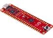
Microchip Technology PIC16F17576 Curiosity Nano Board (EV14L29A)
Designed to evaluate the capabilities of the PIC16F17576, a low-power 8-bit microcontroller (MCU).
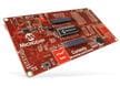
Microchip Technology Curiosity 8-Bit Development Board (DM164137)
Full featured development tool for Microchip 8-pin, 14-pin, and 20-pin 8-bit PIC® Microcontrollers.

Microchip Technology MPLAB® PICkit™ 5 In-Circuit Debugger/Programmer
Enables quick prototyping and portable, production-ready programming for all Microchip components.