Microchip Technology ZL3026x miClockSynth Universal Clock Generators
Microchip ZL3026x miClockSynth Universal Clock Generators distribute several clock frequencies to multiple loads, which improves design reliability, reduces BOM costs, and simplifies a design. The ZL3026x devices create a complex clock tree, replacing several multipliers, synthesizers, and oscillators on a board. With a small package and best-in-class jitter performance, these devices target clock synthesis and frequency conversion applications with tough jitter budgets and tight board space restrictions.Features
- 4x flexible input clocks
- 1x crystal/CMOS input
- 2x differential/CMOS inputs
- 1x single-ended/CMOS input
- Any input frequency from 9.72MHz to 1.25GHz (300MHz maximum for CMOS)
- Activity monitors, automatic/manual switching
- Glitchless clock switching by pin or register
- Automatic self-configuration at power-up from external or internal EEPROM, up to 8x configurations pin-selectable
- External feedback for zero-delay applications
- Numerically controlled oscillator mode
- Spread-spectrum modulation mode
- Generates PCIe 1, 2, 3, and 4 compliant clocks
- Easy-to-configure design requires no external VCXO or loop filter components
- SPI or I2C processor interface
- Core supply voltage options
- 2.5V only
- 3.3V only
- 1.8V+2.5V
- 1.8V+3.3V
- Space-saving 8mm2 QFN-56 with a 0.5mm pitch
- 6x or 10x any frequency, any format outputs
- Any output frequency from 1Hz to 1045MHz
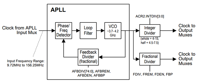
- High-resolution frac-N APLL with 0ppm error (ZL30260-ZL30263)
- APLL has a fractional divider and an integer divider to make 2x independent frequency families (ZL30260-ZL30263)
- 2x fractional-N APLLs with 0ppm error (ZL30264-ZL30267)
- Each APLL has a fractional divider and an integer divider to make a total of 4x independent frequency families (ZL30264-ZL30267)
- Output jitter
- From integer multiply and dividers as low as 0.17ps RMS (12kHz to 20MHz)
- From fractional dividers is typically <1ps RMS, many frequencies <0.5ps RMS
- Each output has an independent divider
- Each output is configurable as LVDS, LVPECL, HCSL, 2xCMOS, or HSTL
- In 2xCMOS mode, the P and N pins can be different frequencies (e.g. 125MHz and 25MHz)
- Multiple output supply voltage banks with CMOS output voltages from 1.5V to 3.3V
- Precise output alignment circuitry and per-output phase adjustment
- Per-output enable/disable and glitchless start/stop (stop high or low)
Applications
- Broadcast video
- Industrial Ethernet networking
- Data centers
- Infotainment
- Human Machine Interfacing (HMI)
Specifications
- Supply voltage
- 2.375V to 3.465V higher core range
- 1.71V to 1.89V lower core range
- 1.71V to 2.625V non-clock I/O pins range
- 1.425V to 2.625V OCx outputs range
- 25MHz to 60MHz crystal oscillation frequency range
- 5pF maximum shunt capacitance, 2pF typical
- 8pF to 16pF load capacitance range, 10pF typical
- 50Ω to 60Ω equivalent series resistance (ESR) range
- 100µW, 200µW, and 300µW maximum crystal drive levels (typical)
- Non-clock CMOS pins
- ±10µA input/output leakage current
- 10pF maximum input capacitance, 3pF typical
- 11pF maximum input hysteresis, 3pF typical
- Clock output on GPIO pin
- 50MHz frequency
- 1.2ns to 2.3ns typical rise/fall time range
- 40% to 60% XA clock input duty cycle range
- Clock inputs
- 0.1V to 1.4V input differential voltage range
- 1.35VDC typical input bias voltage, internally biased)
- Input frequency
- 9.72MHz to 1250MHz differential range
- 9.72MHz to 300MHz single-ended range
- 50kΩ or 80kΩ typical input resistance
- LVDS clock outputs
- 1045MHz maximum frequency
- 1.13V to 1.37V common-mode voltage range
- 310mV to 530mV differential voltage range
- 150ps typical rise/fall time range
- 45% to 55% duty cycle range
- LVPECL clock outputs
- 1045MHz maximum frequency
- Common-mode voltage ranges
- 1.13V to 1.33V when VDDOx = 2.5V
- 1.85V to 2.05V when VDDOx = 3.5V
- 650mV to 1050mV differential voltage range
- 150ps typical rise/fall time range
- 45% to 55% duty cycle range
- HCSL clock outputs
- 250MHz maximum frequency
- 0.6V to 0.95V common-mode voltage range
- 250ps typical rise/fall time range
- 45% to 55% duty cycle range
- CMOS and HSTL (Class I) clock outputs
- 1Hz to 250MHz maximum frequency range
- 0.4ns to 2.2ns typical rise/fall time range
- 42% to 58% duty cycle range
- 300µA typical current when output is disabled
- APLL frequencies
- 3715MHz to 4180MHz VCO range
- 9.72MHz to 156.25MHz PFD input range
- Jitter and skew
- 600kHz typical APLL jitter transfer bandwidth
- 100ps maximum output-to-output skew
- -40°C to +85°C operating temperature range
APLL Block Diagram

Additional Resource
Yayınlandı: 2023-08-18
| Güncellenmiş: 2023-08-22


