Microchip Technology ZL30671LFG7 System Synchronizer
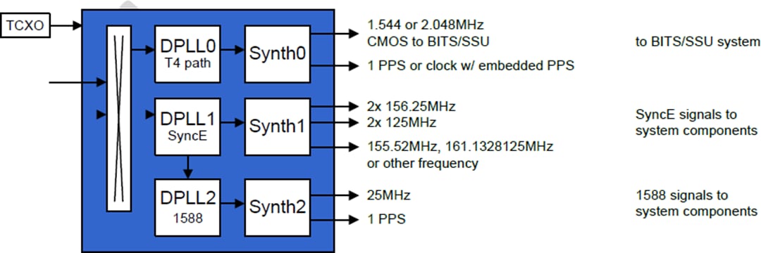
Microchip Technology ZL30671LFG7 System Synchronizer provides 1-, 2-, or 3-channel Synchronous Ethernet (SyncE) packet clock synchronization. This device is optimized for 5G transport and wireless infrastructure equipment using miTimePLL timing technology. The module integrates all features required by a timing card PLL and line card PLL. High integration and ultra-low jitter make this synchronizer ideal for use in chassis-based systems with active and redundant timing cards. The module is suited to single-board applications where a timing device needs to have features of both a timing card and a line card PLL. Microchip Technology ZL30671LFG7 System Synchronizer is available in an LGA-80 package with a -40°C to +85°C operating temperature range.Features
- One, two, or three DPLL channels
- Timing compliance with ITU-T 8262, G.813, G.812, G.8273.2; Telcordia GR-1244, GR-253
- Programmable bandwidth, 1mHz to 470Hz
- Freerun or holdover on the loss of all inputs
- Hitless reference switching
- High-resolution holdover averaging
- Per-DPLL phase adjustment, 1ps resolution
- Programmable tracking range, phase-slope limiting, frequency-change limiting, and other advanced features
- Local oscillator
- Operates from a single TCXO or OCXO: 23.75MHz to 25MHz, 47.5MHz to 50MHz, 114.285MHz to 125MHz
- Very-low-jitter applications can connect a TCXO or OCXO as the stability reference and a low-jitter XO as the jitter reference
- Output clock frequency generation
- Any output frequency from <0.5Hz to 1045MHz (180MHz max for Synth0)
- High-resolution fractional frequency conversion with 0ppm error
- Synthesizers 1 and 2 have an integer and fractional dividers to make a total of 5 frequency families
- Output jitter from Synth 1 and 2 is <0.3ps RMS
- Output jitter from fractional dividers is typically < 1ps RMS, many frequencies <0.5ps RMS
- Each HPOUTP/N pair can be LVDS, LVPECL, HCSL, 2xCMOS, HSTL, or programmable diff.
- In 2xCMOS mode, the P and N pins can be at different frequencies (Example: 125MHz and 25MHz)
- Four output banks, each with a VDDO pin; CMOS output voltages from 1.5V to 3.3V
- Per-synthesizer phase adjust, 1ps resolution
- Per-output programmable duty cycle
- Precise output alignment circuitry and per- output phase adjustment
- Per-output enable/disable and glitchless start/stop (stop high or low)
- Input clocks
- Accepts up to 10 differential or CMOS inputs
- Any input frequency from 5Hz to 900MHz
- Per-input activity and frequency monitoring
- Automatic or manual reference switching
- Revertive or non-revertive switching
- Any input can be a 1PPS SYNC input for REF+SYNC frequency/phase/time locking
- Input-input phase measurement, 1ps resolution
- Input-DPLL phase measurement, 1ps resolution
- Per-input phase adjustment, 1ps resolution
- General features
- Automatic self-configuration at power-up from internal Flash memory
- Input-to-output alignment <200ps (ext feedback)
- Fast REF+SYNC locking for frequency and 1PPS phase alignment with lower-cost oscillator
- Internal compensation (1ppt) for local oscillator frequency error in DPLLs and input monitors
- Numerically controlled oscillator behavior in each DPLL and each fractional output divider
- Easy-to-configure design requires no external VCXO or loop filter components
- 7 GPIO pins with many possible behaviors
- SPI or I2C processor Interface
- 1.8V and 3.3V core VDD voltages
- Power: 3W for 2 inputs, 1 synth, 6 LVDS out
- -40°C to +85°C operating temerpature range
- 11mm x 11mm LGA-80 package
- Lead free
Applications
- Central system timing ICs for SyncE, SyncE+1588, SONET/SDH, OTN, wireless base station, and other carrier-grade systems
- 8262/813 EEC/SEC, Telcordia Stratum 2-4
Block Diagram

Application Example

Yayınlandı: 2022-05-16
| Güncellenmiş: 2023-03-16


