Monolithic Power Systems (MPS) MPQ3438-AEC1 Synchronous Boost Converters
Monolithic Power Systems (MPS) MPQ3438-AEC1 Synchronous Boost Converters are 2.6MHz, quasi-fixed frequency, highly integrated boost converters that operate across a wide 0.8V to 10V input voltage (VIN) range. The MPQ3438 starts up from an input voltage (VST) as low as 2.7V and supports a switching current limit up to 2A with integrated, low-on-resistance [RDS(ON)] power MOSFETs. The MPS MPQ3438 converters come in an AEC-Q100 Grade 1 qualified, QFN-8 (1.5mm x 2mm) package.The MPQ3438 adopts an adaptive constant-off-time (COT) control topology to provide a fast transient response. An internal frequency loop ensures that the operating frequency is fixed in a steady state. The low-side MOSFETs (LS-FET) cycle-by-cycle current limit prevents current runaway, and the high-side MOSFET (HS-FET) eliminates the need for an external Schottky diode. Full protections include configurable input under-voltage lockout (UVLO) and overtemperature protection (OTP).
Features
- Flexible VIN and output voltage (VOUT) operating range
- 2.7V to 10V VST range
- 0.8V to 10V operating VIN
- 1.25 x VIN to 16V VOUT
- Up to 2A switching current limit
- Reduces board size and BOM
- 2.6MHz fixed switching frequency (fSW)
- Available in a QFN-8 (1.5mm x 2mm) package
- Integrated 55mΩ and 100mΩ power MOSFETs
- Adaptive COT control for fast transient responses
- Power-Save Mode (PSM) at light loads
- Internal Soft Start (SS) and compensation
- Frequency foldback for smooth startUp
- Configurable Under-Voltage Lockout (UVLO) and hysteresis
- UVLO, OTP, and OVP protections
- AEC-Q100 Grade 1
- MPSafe™-compatible, functional safety supporting document available
Applications
- Automotive mechanical power supplies
- Automotive LED drivers
- Automotive infotainment
Specifications
- 2.7V to 10V start-up input voltage range
- 0.8V to 10V operating input voltage range
- 0.9V to 10V start-up input voltage with VCC bias (VST2)
- 3.6V maximum external VCC bias voltage
- 2μA maximum shutdown current
- 2.6MHz typical switching frequency
- 1.7A to 2.7A switching current limit range
- 30A maximum HS-FET body diode inrush current
- 2.1W maximum continuous power dissipation
- Thermal protection
- +165°C thermal shutdown
- +25°C thermal shutdown hysteresis
- ESD ratings
- Class 2 Human Body Model (HBM)
- Class C2b Charged-Device Model (CDM)
- -40°C to +125°C operating junction temperature range
- +150°C maximum junction temperature
- +260°C maximum lead temperature
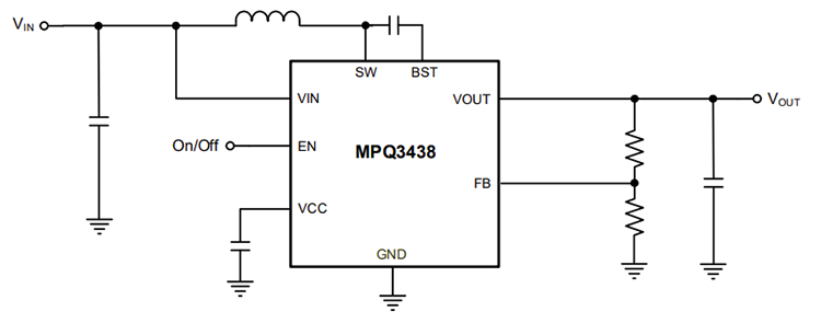
Typical Application Circuit

Functional Block Diagram

Yayınlandı: 2025-03-20
| Güncellenmiş: 2025-03-26


