


Texas Instruments LM516x/LM516x-Q1 Synchronous Buck Converters
Texas Instruments LM516x/LM516x-Q1 Synchronous Buck Converters are designed to regulate over a wide input voltage range, minimizing the need for external surge suppression components. A minimum controllable on-time of 50ns facilitates large step-down conversion ratios, enabling the direct step-down from a 48V nominal input to low-voltage rails for reduced system complexity and solution cost. The LM516x/LM516x-Q1 operates during input voltage dips as low as 6V, at nearly 100% duty cycle if needed, making it an excellent choice for wide input supply range industrial and high-cell count battery pack applications.
With integrated high-side and low-side power MOSFETs, the LM5169/LM5169-Q1 delivers up to 0.65A of output current, and the Texas Instruments LM5168/LM5168-Q1 delivers up to 0.3A of output current. A constant on-time (COT) control architecture provides a nearly constant switching frequency with excellent load and line transient response. The LM516x/LM516x-Q1 is available in FPWM or auto mode operation. FPWM mode provides forced CCM operation across the entire load range, supporting an isolated fly-buck operation. The auto mode enables ultra-low IQ and diode emulation mode operation for high light-load efficiency. The LM516x-Q1 devices are AEC-Q100 qualified for automotive applications.
Features
- Designed for reliability in rugged applications
- Wide input voltage range of 6V to 120V
- -40°C to +150°C junction temperature range
- Fixed 3ms internal soft-start timer
- Peak and valley current-limit protection
- Input UVLO and thermal shutdown protection
- Suited for scalable industrial power supplies and battery packs
- Low minimum on and off times of 50ns
- Adjustable switching frequency up to 1MHz
- Diode emulation for high light-load efficiency
- Auto mode with low quiescent current (< 10µA)
- FPWM mode enables a fly-buck capability
- 3µA shutdown quiescent current
- Pin-to-pin compatible with LM5164, LM5163, LM5017, and LM34927
- Integration reduces solution size and cost
- COT mode control architecture
- Integrated 1.9Ω NFET buck switch
- Integrated 0.71Ω NFET synchronous rectifier
- 1.2V internal voltage reference
- No loop compensation components
- Internal VCC bias regulator and boot diode
- Open-drain power-good indicator
- 8-pin SOIC package with PowerPAD
Applications
- Communications – brick power module
- Industrial battery pack (≥ 10S)
- Battery pack – e-bike/e-scooter/LEV
Functional Block Diagram

Development Tools

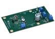
Texas Instruments LM5168PEVM Regulator Evaluation Module (EVM)
Fully assembled and tested circuit for evaluating the LM5168P, a 115V DC/DC fly-buck regulator.
Texas Instruments LM5168FEVM Converter Evaluation Module (EVM)
A fully assembled and tested circuit for evaluating the LM5168, a 115V DC/DC fly-buck regulator.

Texas Instruments LM5169FEVM Evaluation Module
Implements the LM5169FNGUR to create a 10V output capable with 300mA load on the primary side.

Texas Instruments LM5169PEVM Converter Evaluation Module (EVM)
Evaluates the LM5169P, a 115V DC-DC buck regulator that achieves high conversion efficiency.